Primary Category | Specific Item | Core Description | Key Details and Specifications |
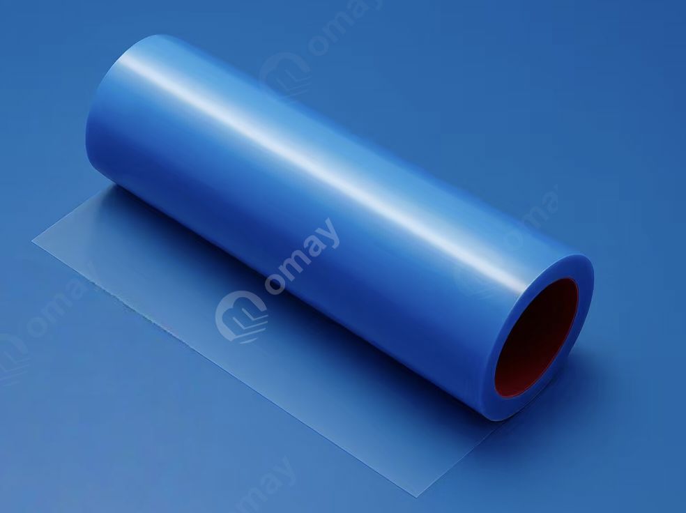
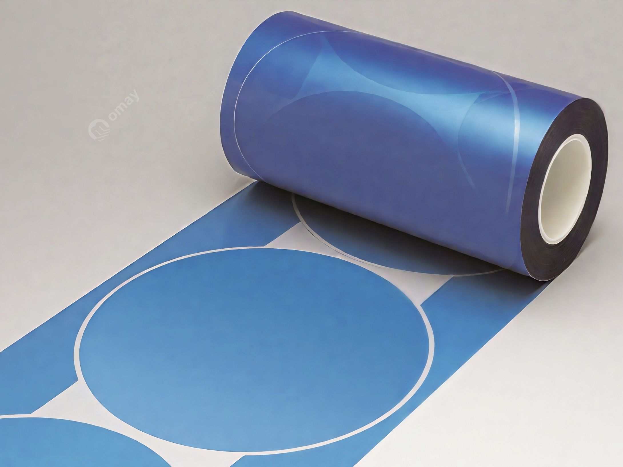
Base film materials (CPE and PP) | Chlorinated polyethylene (CPE) film | A high-performance film with strong chemical resistance and excellent mechanical durability, optimized for precision protection. | - Chemical Resistance: High resistance to a wide range of chemicals, suitable for demanding processing environments - Durability: Good mechanical strength, able to withstand physical stress - Transparency: High optical clarity, suitable for wafer surface protection and inspection |
Polypropylene (PP) film | A film with balanced performance and high cost-effectiveness, meeting general protection needs. | - Cost-effectiveness: More economical than specialty films, suitable for high-volume, cost-sensitive applications - Transparency: Moderate optical clarity, meeting the visual requirements of most semiconductor processes - Temperature resistance: Reliable performance in medium and low temperature environments |
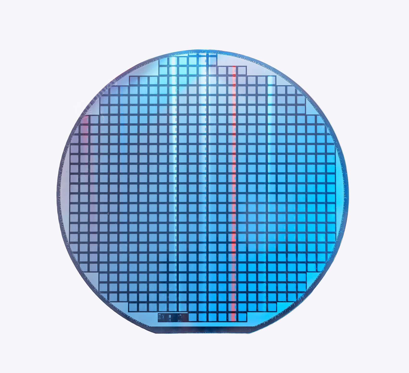
Key protective and functional properties | High transparency and clarity | Ensures the protected surface (e.g., wafer) is clearly visible, which is essential for quality control. | - Enables clear inspection of the wafer surface during dicing and handling - Keeps surface details (e.g., defects, patterns) visible for precision quality inspection |
Excellent adhesion | Strong adhesion firmly fixes the film to the target surface (e.g., wafer) without displacement. | - Prevents shifting or peeling during processing, handling, or transportation - Provides stable and reliable protection throughout the production process |
Protection against mechanical damage | Protects fragile surfaces (e.g., wafers, electronic components) from physical damage. | - Resistant to scratches, impact, and abrasion during dicing, handling, and storage - Keeping sensitive surfaces (such as semiconductor wafers) intact and avoiding process failures |
Contamination Prevention | Preventing particulate contaminants from depositing on protected surfaces. | - Preventing dust, dirt and other impurities from adhering to wafer or component surfaces - Maintain cleanliness and precision, which are critical for semiconductor manufacturing and electronic assembly |
Temperature and chemical resistance | Resistance levels vary by material type and can accommodate diverse processing conditions. | - Temperature resistance: PP is suitable for medium and low temperature environments; CPE may offer stronger resistance (depending on the material) - Chemical Resistance: CPE offers strong chemical resistance; PP provides basic protection (depending on the application) - Adapt to different processing environments (e.g., chemical cleaning, temperature-controlled storage) |
Easy to apply, easy to remove | Simple to handle with minimal residue after use. | - Efficient application, helping to streamline production processes - Clean removal with minimal residue, preventing surface contamination or damage after protection ends |
Application Scenarios | Semiconductor manufacturing | Provides essential protection for wafers during key production steps. | - Wafer dicing: Prevent surface damage and ensure dicing precision - Wafer handling and storage: Keep wafers intact during transport and storage, ensuring quality for subsequent processes |
Electronic Component Protection | Used in the production and assembly of electronic components. | - Protect precision electronic components (such as microchips and sensors) from damage and contamination during manufacturing and assembly - Keep surfaces clean to ensure reliable component performance |
Laboratory & R&D | Protect samples and reagents in controlled environments. | - Prevent laboratory samples and reagents from contamination to ensure accurate experimental results - Prevent physical damage to sensitive R&D materials (such as prototype parts) |
Eco-Friendly & Safety Features | Eco-Friendly Options | Recyclable products are available (depending on material) to support sustainability goals. | - Use recyclable formulations to reduce plastic waste - Support eco-friendly practices in industrial and laboratory environments (availability varies by material type) |
Safety & Compliance | Manufactured with non-toxic materials and compliant with industrial safety standards. | - Comply with safety regulations for electronic and industrial applications - Eliminate the risk of toxic contamination to protected surfaces (such as wafers and components) or laboratory samples |












 Home



 Su Gong Wang An Bei No. 19046638



 中文
 English
 Español
 العربية